Shenzhen Chenkun Vision Technology Co.,Ltd.

Unveiling the Power of CK Vision's SPI Camera: Innovation at its Finest

Table of Content [Hide]

    SPI Camera Integration Guide

    An SPI camera module is designed for embedded systems that need compact imaging hardware and a serial connection to a microcontroller or processor. Successful integration depends on more than connecting the clock and data pins. Engineers must confirm the module protocol, SPI clock, image format, frame size, memory capacity, DMA support and the actual frame rate required by the application.

    This guide explains how SPI camera modules work, how to estimate image-transfer bandwidth and frame-buffer memory, and what information should be verified before developing a prototype. It focuses on MCU-based embedded imaging rather than home surveillance or concealed-monitoring applications.

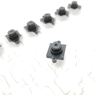
    For a product-level reference, CK Vision’s  0.3MP SPI camera module uses the GC032A image sensor and provides VGA-class imaging for compact embedded devices. The final host-side frame rate and image format must still be confirmed against the selected MCU and firmware architecture.

    What Is an SPI Camera Module?

    SPI stands for Serial Peripheral Interface. It is a synchronous serial connection commonly used for short-distance communication between a host processor and peripheral devices. A typical SPI connection may include a serial clock, chip-select signal and one or more data lines. However, SPI camera implementations are not universally identical.

    Depending on the camera architecture, SPI may be used to configure the camera, transfer image data, or communicate with an intermediate controller or image processor. Therefore, the term “SPI camera” alone does not confirm the electrical pinout, command structure or maximum data-transfer rate.

    Important:  A sensor specification such as 640 × 480 at 30 fps describes a supported sensor mode. It does not automatically prove that the complete module can deliver uncompressed VGA video through SPI to every MCU at 30 fps.

    How an SPI Camera Connects to an MCU

    Image Sensor
    Captures the image
    Camera Processing
    Formats image data
    SPI Transfer
    Clock and data
    MCU Buffer
    Receives frame data
    Application
    Display or analysis

    The MCU may receive an entire frame, several image lines at a time, or smaller data blocks. The most appropriate architecture depends on available RAM, SPI speed, DMA capability and whether the application needs to display, store or analyze the image.

    Before PCB design begins, confirm the camera’s voltage levels, SPI mode, clock limit, chip-select behavior, reset timing, frame-start indication, packet structure and error-handling method. General SPI background is available in this  Analog Devices SPI application note.

    Calculate SPI Camera Bandwidth Before Selecting the MCU

    A simplified calculation for uncompressed image payload is:

    Width × Height × Bits per Pixel × Frames per Second

    RGB565 and YCbCr 4:2:2 normally require 16 bits per pixel. A 640 × 480 RGB565 image therefore contains 614,400 bytes of uncompressed pixel data. The following figures represent image payload only and do not include command bytes, packet headers, blanking, retries or other implementation overhead.

    Image ModeFormat AssumptionFrame RatePayload Rate
    320 × 240RGB565, 16 bpp10 fpsApproximately 12.3 Mbps
    320 × 240RGB565, 16 bpp30 fpsApproximately 36.9 Mbps
    640 × 480RGB565, 16 bpp5 fpsApproximately 24.6 Mbps
    640 × 480RGB565, 16 bpp10 fpsApproximately 49.2 Mbps
    640 × 480RGB565, 16 bpp30 fpsApproximately 147.5 Mbps

    Engineering conclusion: If the calculated payload approaches or exceeds the practical SPI throughput of the MCU, reduce the resolution or frame rate, use a smaller region of interest, select a different image format, add buffering or evaluate another camera interface. Do not approve the design based only on the sensor’s maximum frame-rate specification.

    Frame-Buffer Memory Requirements

    Memory is often the first limitation in a small MCU imaging system. A complete 640 × 480 RGB565 frame requires approximately 600 KiB of storage. Double buffering requires roughly twice that amount before application memory, display buffers and software overhead are considered.

    Buffer StrategyAdvantageMain Consideration
    Full-frame bufferSimplifies complete-frame processingRequires sufficient internal or external RAM
    Double bufferingAllows capture and processing to overlapApproximately doubles frame memory
    Line bufferSignificantly reduces RAM requirementsProcessing must keep pace with incoming data
    External memorySupports larger frames and more processingAdds PCB space, cost and memory bandwidth requirements

    DMA is especially valuable because it can move SPI data into memory with less continuous CPU involvement. The MCU must still process or release each buffer before the next image block arrives, otherwise frames may be incomplete or dropped.

    Choosing the Image Output Format

    The selected image format affects bandwidth, memory consumption and software complexity. CK Vision’s CK-032A-V2.0 product specification lists YCbCr 4:2:2, RGB565 and Raw Bayer output options. Availability should be confirmed for the final firmware and operating mode.

    RGB565

    Uses 16 bits per pixel and can simplify integration with many embedded displays. Confirm color order, byte order and display-controller compatibility.

    YCbCr 4:2:2

    Separates luminance and color information and is useful for video-oriented processing. The host must support the actual byte sequence used by the module.

    Raw Bayer

    Preserves sensor-level pixel information but requires demosaicing and additional image processing. Confirm the Bayer pattern, bit depth and packing method.

    SPI Camera vs MIPI CSI-2 and USB Camera

    SPI, MIPI CSI-2 and USB represent different integration strategies. This section provides only a brief distinction so that this article does not compete with CK Vision’s dedicated USB camera vs MIPI CSI-2 camera guide .

    InterfaceTypical HostMain StrengthMain Limitation
    SPIMCU or compact processorLow pin count and MCU-oriented integrationImage throughput and memory must be carefully calculated
    MIPI CSI-2Application processor or imaging SoCHigh-speed sensor-to-processor image transferRequires compatible CSI receiver, driver and ISP pipeline
    USBPC, industrial computer or embedded USB hostStandardized host connection on UVC-compatible modulesRequires bridge electronics and USB host support

    The MIPI Alliance describes  MIPI CSI-2  as a high-speed embedded imaging interface for transferring still and video data from image sensors to application processors. SPI is generally better evaluated separately for MCU-oriented, lower-data-rate designs.

    SPI Camera Module Integration Checklist

    1. Electrical compatibilityConfirm I/O voltage, power rails, grounding, reset signals and power-up sequence.
    2. SPI configurationConfirm clock polarity, clock phase, bit order, clock limit and chip-select timing.
    3. Transfer protocolObtain the command set, packet format, frame boundaries and error-handling rules.
    4. BandwidthCalculate payload using the required resolution, format and sustained frame rate.
    5. Memory architecture  Decide whether the MCU will use a frame buffer, double buffer, line buffer or external RAM.
    6. Software processingConfirm DMA, pixel conversion, display, storage and image-analysis requirements.
    7. Optical requirementsDefine working distance, FOV, distortion, focus range and enclosure window.
    8. Prototype validationTest continuous capture, frame loss, image stability, temperature and power behavior.

    Suitable Applications for an SPI Camera

    SPI camera modules are most practical when the application prioritizes compact size, controlled image requirements and MCU integration over high-resolution continuous video.

    • Barcode and QR readers: compact image capture for decoding within a controlled working distance.

    • Scanning pens: line-by-line or small-region image acquisition for text-recognition workflows.

    • Educational devices and toys: low-resolution visual input on a cost- and power-constrained platform.

    • Compact handheld instruments: image preview, documentation or simple visual inspection.

    • Low-power IoT devices: periodic image acquisition rather than continuous high-resolution streaming.

    • Embedded recognition terminals: controlled image capture where the MCU and algorithm can operate within the available bandwidth.

    Common SPI Camera Integration Problems

    ProblemPossible CauseRecommended Check
    No camera responsePower, reset, SPI mode or chip-select errorMeasure power rails and inspect SPI timing with a logic analyzer
    Incomplete imageBuffer overflow, lost packet or incorrect frame lengthCheck DMA completion, packet count and frame boundaries
    Wrong colorsIncorrect pixel order, byte order or Bayer patternVerify the selected format and host-side conversion
    Low frame rateSPI throughput, CPU load or memory-write limitationMeasure sustained transfer rate and reduce processing during capture
    Intermittent errorsSignal integrity, grounding, cable length or clock timingReview layout, grounding, clock edge quality and operating temperature

    Information Required for an SPI Camera Sample

    To evaluate a standard or customized SPI camera module, provide the following information:

    • MCU, processor or development-board model;

    • Available SPI clock and supported SPI modes;

    • Required resolution and sustained frame rate;

    • Required RGB, YCbCr or Raw Bayer output;

    • Available internal and external memory;

    • Display, storage or image-analysis requirement;

    • PCB size, FPC, connector and pinout requirements;

    • Working distance, field of view and focus requirement;

    • Power-supply and operating-temperature conditions;

    • Prototype quantity and expected production demand.

    Frequently Asked Questions

    Is an SPI camera the same as a MIPI camera?

    No. SPI is commonly used with MCUs and lower-data-rate peripheral communication. MIPI CSI-2 is a dedicated high-speed imaging interface generally connected to an application processor with a compatible CSI receiver.

    Can an SPI camera transmit 640 × 480 video at 30 fps?

    It depends on the output format, actual SPI data rate, transfer protocol and host architecture. Uncompressed 640 × 480 RGB565 at 30 fps requires approximately 147.5 Mbps of image payload before protocol overhead, so sensor-mode support does not guarantee delivery through every SPI host.

    Does an MCU need enough RAM for a complete image?

    Not always. Some designs process data through line buffers or smaller blocks. Full-frame processing, rotation, storage and many recognition algorithms may require a complete frame buffer or external memory.

    Which image format is easiest for an embedded display?

    RGB565 can simplify integration with displays that accept the same pixel format. The final choice depends on the camera output, display controller, memory capacity and whether additional image processing is required.

    Can an SPI camera module work with any microcontroller?

    Not automatically. The MCU must provide compatible voltage levels, SPI timing, adequate sustained throughput, sufficient memory and suitable software support. Compatibility should be validated with the exact module and host board.

    Can the PCB, FPC, connector and lens be customized?

    Customization can be evaluated according to the enclosure, connector, pinout, working distance, FOV and production requirements. Electrical and software compatibility must be reviewed before confirming a customized configuration.

    Conclusion

    An SPI camera module can provide a compact imaging solution for MCU-based devices, but successful integration requires careful bandwidth, memory and protocol planning. Resolution and sensor frame rate should not be evaluated independently from the SPI clock, image format, frame-buffer architecture and host processing load.

    Calculate the required image payload first, confirm the module’s electrical and communication specifications, and test the complete camera, MCU, firmware and optical configuration under real operating conditions before approving the design.

    Need an SPI Camera Module for Your Embedded Project?

    Send CK Vision your MCU model, required resolution, frame rate, output format, SPI configuration, memory capacity, enclosure drawing and optical requirements for compatibility evaluation.

                   Contact CK Vision                                        View the 0.3MP SPI Camera Module            

    References